Beyond Silicon: How Atom-Thin Materials Are Revolutionizing Chips
Technology tamfitronics
An artist’s depiction of a missing chalcogen atom in the middle layer of a bulk transition-metal dichalcogenide. Credit: Kyle Palmer / PPPL Communications Department
New research boosts our understanding of a likely candidate for next-generation computer chips.
Scientists at the Princeton Plasma Physics Laboratory are advancing semiconductor technology by developing thinner, more efficient materials called transition-metal dichalcogenides (TMDs). These materials, only a few atoms thick, could lead to more compact and powerful computer chips. The research also investigates the role of defects within these materials, which can affect their electrical properties and potentially enhance their functionality.
The Evolution of Computer Chips
Silicon computer chips have served us well for more than half a century. The tiniest features on chips currently sold are approximately 3 nanometers — a startlingly small size given that a human hair is roughly 80,000 nanometers wide. Reducing the size of features on chips will help us meet our endless need for more memory and processing power in the palm of our hand. But the limit of what can be achieved with standard materials and processes is near.
Breakthroughs in Chip Materials
Researchers at the U.S. Department of Energy’s (DOE) Princeton Plasma Physics Laboratory (
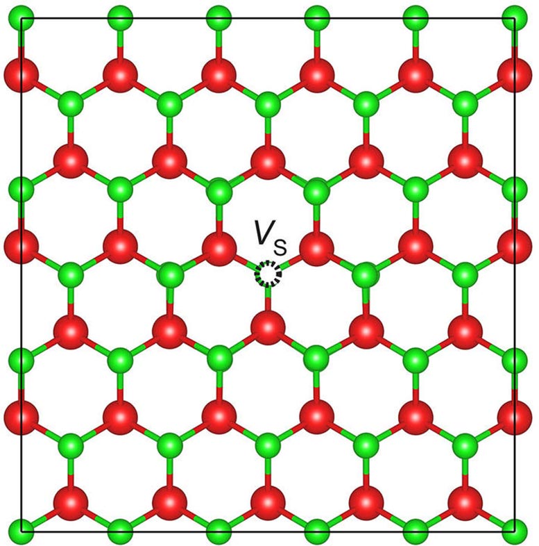
This model shows the spot where the missing chalcogen atoms should be, as represented by the black circle in the center of an otherwise undisturbed pattern of atoms. This view looks down on the middle layer of the TMD. Credit: Shoaib Khalid, Bharat Medasani and Anderson Janotti / PPPL and the University of Delaware
Research Insights on Chalcogen Vacancies
The other type of defect explored in the paper is known as a chalcogen vacancy: a missing atom of oxygen, sulfur, selenium or tellurium, depending on the type of TMD. The researchers focused on explaining the results of past experiments on flakes of the bulk TMD material molybdenum disulfide. The experiments, which involved shining light on the TMD, showed unexpected frequencies of light coming from the TMD. These unexpected frequencies, the researchers found, could be explained by the movement of electrons related to the chalcogen vacancy.
“This is a common defect. They can often see it from the images of scanning tunneling microscopes when they grow the TMD film,” Khalid said. “Our work provides a strategy to investigate the presence of these vacancies in the bulk TMDs. We explained past experimental results shown in molybdenum disulfide, and then we predicted a similar thing for other TMDs.”
The process suggested by the researchers involves analyzing the TMD for defects using measurement techniques called photoluminescence to see which frequencies of light are emitted by the material. The peak frequency of light can be used to determine the electron configurations of the atoms in the TMD and the presence of chalcogen defects. The journal article includes information about the frequencies that would be emitted by five types of TMDs with chalcogen vacancies, including molybdenum disulfide. The results, therefore, provide a guideline for investigating chalcogen vacancies in future experiments.
Reference: “Role of chalcogen vacancies and hydrogen in the optical and electrical properties of bulk transition-metal dichalcogenides” by Shoaib Khalid, Anderson Janotti and Bharat Medasani, 24 May 2024, 2D Materials.
DOI: 10.1088/2053-1583/ad4720
This work was supported by the DOE under grant DE-AC02-09CH11466 and the National Science Foundation (NSF) award #OIA-2217786. Calculations were carried out at the National Energy Research Scientific Computing Center (NESRC) under contract number DE-AC02-05CH11231 using NERSC award BES-ERCAP27253, the Stellar cluster at
Discover more from Tamfis Nigeria Lmited
Subscribe to get the latest posts sent to your email.


 Hot Deals
 Shopfinish
 Shop
Shop Appliances
 Babies & Kids
 Best Selling
 Books
Books Consumer Electronics
 Furniture
 Home & Kitchen
 Jewelry
 Luxury & Beauty
 Shoes
Shoes Training & Certifications
 Wears & Clothings


